TRENDING HASHTAG: #substrate
Trending Posts
-
CRYSCORE OPTOELECTRONIC LIMITED Wind Zhu
STANDARD SAPPHIRE WAFERS (C-PLANE)
#c #plane #sapphire #substrate
CRYSCORE can offer Epi-Ready grade sapphire wafer with a very low surface roughness in complete orientation options.
C-plane(0001) sapphire wafers are being... moreSTANDARD SAPPHIRE WAFERS (C-PLANE)
#c #plane #sapphire #substrate
CRYSCORE can offer Epi-Ready grade sapphire wafer with a very low surface roughness in complete orientation options.
C-plane(0001) sapphire wafers are being extensively used for epitaxial growth of III-V and II-VI compounds, such as gallium nitride (GaN), aluminum nitride (AlN), for bright blue and green LED and laser diodes.
Technical Applications of Standard Sapphire Wafers
C-plane sapphire wafers are widely used to grow III-V and II-VI deposited films of wide band-gap nitride and oxide semiconductor materials such as gallium nitride (GaN), aluminum nitride (AlN), indium nitride (InN), zinc oxide (ZnO ultraviolet light emission) and tin oxide (SnO2 ultraviolet luminescent material), etc.
In addition, standard C-plane(0001) sapphire wafers are widely applied to fabricate LED white and blue light, ultraviolet and deep UV LED epitaxial wafers by Metal-Organic Vapor Deposition(MOCVD), Molecular Beam Epitaxy (MBE), Plasma Enhanced Chemical Vapor Deposition(PECVD) and other epitaxy growth methods.
CRYSCORE standard sapphire wafers also are used as the substrates of heterojunction bipolar transistor (HBT), a laser diode (LD), UV detector, nanotube, and the heat dissipation material of high temperature and high power high-frequency electronic device.
Competitive Advantages of CRYSCORE's Sapphire Wafers
99.999 % high purity single crystal Al2O3 material.
Special CMP (Chemical Mechanical Polishing) technology to ensure its performance at a low cost.
Excellent surface quality in all orientations (less than 0.2 nm for C-plane, less than 0.5 nm for A-plane, M-plane, R-plane, N-plane, V-plane, 10-14, etc.)
Cleaned in class 100 cleanroom by ultrapure water with quality above 18MΩ *cm.
25 pcs a pack or single pack is available to maximize customer flexibility in their research.
Traceable product serial number.
Compact carton packaging for safer shipping and cost-saving.
Standard wafers are Generally in stock to ensure a quick delivery. less
September 21, 2020

We are a reliable c plane sapphire wafer manufacturer & supplier. CRYSCORE can produce 2-inch to 8-inch C plane single side and double side polished standard sapphire wafers with lower cost, steady physical and chemical properties. Please contact us: sapph
-
CRYSCORE OPTOELECTRONIC LIMITED Wind Zhu
STANDARD SAPPHIRE WAFERS (C-PLANE)
#c #plane #sapphire #substrate
CRYSCORE can offer Epi-Ready grade sapphire wafer with a very low surface roughness in complete orientation options.
C-plane(0001) sapphire wafers are being... moreSTANDARD SAPPHIRE WAFERS (C-PLANE)
#c #plane #sapphire #substrate
CRYSCORE can offer Epi-Ready grade sapphire wafer with a very low surface roughness in complete orientation options.
C-plane(0001) sapphire wafers are being extensively used for epitaxial growth of III-V and II-VI compounds, such as gallium nitride (GaN), aluminum nitride (AlN), for bright blue and green LED and laser diodes.
Technical Applications of Standard Sapphire Wafers
C-plane sapphire wafers are widely used to grow III-V and II-VI deposited films of wide band-gap nitride and oxide semiconductor materials such as gallium nitride (GaN), aluminum nitride (AlN), indium nitride (InN), zinc oxide (ZnO ultraviolet light emission) and tin oxide (SnO2 ultraviolet luminescent material), etc.
In addition, standard C-plane(0001) sapphire wafers are widely applied to fabricate LED white and blue light, ultraviolet and deep UV LED epitaxial wafers by Metal-Organic Vapor Deposition(MOCVD), Molecular Beam Epitaxy (MBE), Plasma Enhanced Chemical Vapor Deposition(PECVD) and other epitaxy growth methods.
CRYSCORE standard sapphire wafers also are used as the substrates of heterojunction bipolar transistor (HBT), a laser diode (LD), UV detector, nanotube, and the heat dissipation material of high temperature and high power high-frequency electronic device.
Competitive Advantages of CRYSCORE's Sapphire Wafers
99.999 % high purity single crystal Al2O3 material.
Special CMP (Chemical Mechanical Polishing) technology to ensure its performance at a low cost.
Excellent surface quality in all orientations (less than 0.2 nm for C-plane, less than 0.5 nm for A-plane, M-plane, R-plane, N-plane, V-plane, 10-14, etc.)
Cleaned in class 100 cleanroom by ultrapure water with quality above 18MΩ *cm.
25 pcs a pack or single pack is available to maximize customer flexibility in their research.
Traceable product serial number.
Compact carton packaging for safer shipping and cost-saving.
Standard wafers are Generally in stock to ensure a quick delivery. less
September 21, 2020

We are a reliable c plane sapphire wafer manufacturer & supplier. CRYSCORE can produce 2-inch to 8-inch C plane single side and double side polished standard sapphire wafers with lower cost, steady physical and chemical properties. Please contact us: sapph
Do you want to report this? Why didn't you like it?

-
CRYSCORE OPTOELECTRONIC LIMITED Wind Zhu
PATTERNED SAPPHIRE SUBSTRATES
#sapphire #substrate #manufacturers
Sapphire wafer is the most widely used substrate material in semiconductor lighting industry, and patterned sapphire substrate... morePATTERNED SAPPHIRE SUBSTRATES
#sapphire #substrate #manufacturers
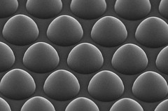
Sapphire wafer is the most widely used substrate material in semiconductor lighting industry, and patterned sapphire substrate (short for PSS) is the general method to improve the luminous efficiency of semiconductor lighting devices. These sapphire substrates are with periodic structures of various shapes such as cone, dome, pyramid, and pillar, etc.
Cryscore's Excellent Patterned Sapphire Substrates
Pattern dimension, aspect ratio, and uniformity across the wafer as well as consistency from wafer to wafer, are important factors to improve the light extraction. Currently, we provide 2-inch and 4-inch patterned sapphire substrates (PSS sapphire and wafer) with the following specifications. Diameter: 2.7 +/- 0.1 μm. Spacing: 0.3 +/- 0.1 μm. Depth: 1.7 +/- 0.15 μm.
2 Inch Patterned Sapphire Substrates
PSS is to design and manufacture specific nano-scale microstructure pattern on sapphire substrate.
4 Inch Patterned Sapphire Substrates
Patterned Sapphire Substrates (PSS) is micro-patterned sapphire substrate used to for GaN based light emitting diodes(LEDS). less
September 21, 2020

Browse pss sapphire at cryscor.com. It can improve the luminous efficiency of semiconductor lighting devices and has two sizes available - 2 inch/4 inch Patterned Sapphire Substrates. Quote now & get patterned sapphire substrates price!
Loading ...
Updates

Loading ...

Loading ...
There are no more results to show.
 Find in Members
 Find in Projects
 Find in Channels